Miracle Material
It has been hailed as a wonder material full of suprising, often counterintuitive properties, one of the most versatile materials ever to spring from the engineering lab. Tougher than steel, a whisper-thin coating can superconduct electricity at room temperature, mend itself, and change properties according to whatever it’s wrapped around, including metal. Corrosion could disappear “almost like magic,” predicts MIT chemical engineering Prof. Michael Strano.
Isolated just eight years ago by researchers at Britain’s University of Manchester, this single-layer lattice of carbon atoms has fast become the stuff of legend. Its potential seems boundless, from sensors that detect mere molecules of poison gas to carbon fiber replacements and even the next Teflon. Thanks to its ability to conduct electricity some 100 times as fast as silicon, the foundation of integrated circuits, it could come to define 21st-century computing.
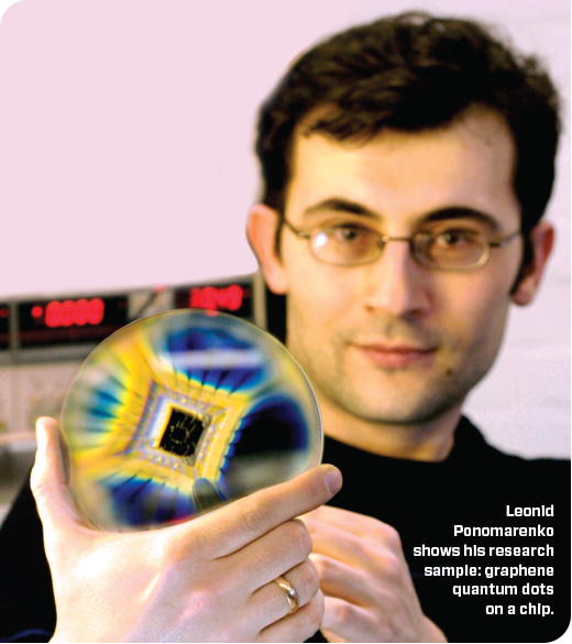
Are claims for graphene overblown? Mark Hersam, a professor of materials science and engineering at Northwestern University, is “worried about a graphene bubble.” Still, he notes, with so many wide-ranging potential applications, “if only one or two pan out, that would justify the excitement.” More bullish is Leonid Ponomarenko, a physicist at Manchester who works closely with the two physicists who won a Nobel Prize for isolating graphene, Andre Geim and Konstantin Novoselov. “No other material has such a diverse combination of properties,” says Ponomarenko. “And that’s what makes this material unique.”
Graphene actually encompasses a “huge variety of materials that have emerged and continue emerging,” as Geim noted in an email to Prism. These include graphene in many layers with varying properties, as well as graphene cousins, such as graphene oxide, graphane, and fluorographene. “If graphene does not work for a particular project, the counterparts come to the rescue,” explains Geim. “This assures not a single, not a hundred, but a cornucopia of graphene incarnations. Just as with plastics, one name covers many items.”
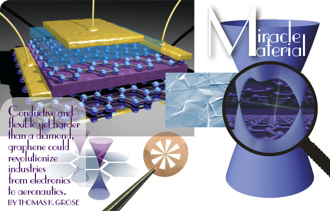
Even in pure form, graphene has properties as varied as they are contradictory. The lightest material yet discovered, it’s highly flexible and stretchable. But it’s also the strongest material on Earth — harder than a diamond and some 200 times as sturdy as steel. Graphene is the world’s most effective conductor of heat, more transparent than glass, and the thinnest material there is, though nothing is more impermeable. These diverse properties give engineers a lot to play with, which is why graphene is expected to revolutionize many industries, including electronics, energy, medicine, transportation, and aeronautics.
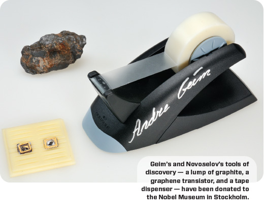
Ironically, this miracle material springs from mundane stock: graphite, or common pencil lead. Graphene’s structure was first theorized in 1947 but thought not to exist in nature. Then, in 2004, Geim and Novoselov took a small chunk of graphite and began peeling it apart, layer by layer, using cellophane tape. Eventually, they whittled down to a single, one atom-thick layer that, when viewed under an electron microscope, looked like a sheet of carbon atoms arranged in a neat, repeating honeycomb pattern, like chicken wire. The discovery kick-started a science and engineering revolution. In 2005, just three published papers discussed graphene; by 2010, that number had soared to 3,000.
The first big commercial uses of graphene are most apt to be in high-value goods that can accommodate the cost of the material and don’t necessarily require pristine versions. Likely candidates include touch-screens, conductive ink for electronic printing, batteries and capacitors, flexible electronic devices, and solar cells. Yun Hang Hu, an associate professor of materials science and engineering at Michigan Tech, has mixed graphene with titanium dioxide to make dye-sensitized solar cells that are 52.4 percent better at converting light into electricity than current versions. “It is a very simple procedure, and commercially it would be easy to do,” Hu says. Graphene might also some day revolutionize fiber-optic telecommunications. Engineers at Columbia University, working with researchers at Singapore’s Institute of Microelectronics, recently created a graphene-silicon hybrid device that eventually could be used for ultralow-power, on-chip communications. Adding graphene crystals transforms crystals of silicon from a passive material into one that can generate microwave photonic signals and perform the conversion of photonic wavelengths at levels needed for faster, more efficient telecommunications. The material is also optically nonlinear, which means it can be switched on and off, a property required for digital telecommunications.
Graphene must overcome two major hurdles before claiming superstar status, however. First, there is still no way to mass-produce graphene economically. Second, graphene conducts electricity so well that there’s no way to turn off the current, which hampers its use in integrated circuits. Like most conductors, graphene lacks a band gap that separates the conductor and valance bands. Electrons move freely through them but can’t be switched off, a function that is crucial to the binary operations of computers. Moreover, a chip laden with graphene transistors packed tightly together would leak so much current that it would melt almost instantaneously.
Dry Ice & Stainless Steel
The most pristine graphene still comes from micromechanical exfoliation – otherwise known as the Scotch tape method – which is hardly practical for industrial-scale production. Another method sprays a carbon-based chemical vapor on a substrate, usually copper, under high temperatures. While the quality is not bad, “it is expensive and difficult to grow in large areas,” says Junhong Chen, a mechanical engineering professor at the University of Wisconsin, Milwaukee.
Breakthroughs may loom, however. Researchers at Case Western Reserve University and South Korea’s Ulsan National Institute of Science and Technology claim their method can produce large quantities of quality graphene cheaply. They mix graphite and dry ice in a ball miller canister containing stainless steel balls. The resulting flakes are dispersed in a solvent, where they form sheets of graphene. The flakes and a solvent can also be placed on a piece of silicon and then heated to produce a thin film of graphene. Liming Dai, a professor of macromolecular science and engineering at Case Western, says the resulting graphene “is almost as conductive” as pure graphene made with sticky tape. He’s convinced the method can yield large amounts of graphene in pieces of up to 10 to 14 inches, perfect for computer touchscreens. “Ball milling is an inexpensive process, and we don’t use expensive chemicals,” Dai adds.
There’s still the problem of introducing a band gap for use in computer chips. Possible solutions include a chemical treatment to create an insulating gap. The so-called Hummer’s method, first developed in 1957, uses harsh acids on graphite to produce the insulator graphene oxide, or GO. A second chemical bath changes the GO to graphene, though in a version that’s less conductive because the acids damage the delicate lattice of carbon atoms. More recently, Hersam’s group at Northwestern has oxidized graphene in an ultrahigh vacuum chamber containing a superhot tungsten filament. Researchers pump oxygen into the chamber, and the heat splits the molecules into oxygen atoms that insert themselves into the graphene lattice. The resulting material is highly homogenous, and the oxidation process is reversible. Further tests will prove if it has opened up a sufficient energy gap, and if it preserves the flow of electrons. “It’s a significant advance chemically, but it remains to be seen if it’s an application advance,” Hersam says.
Meanwhile, Chen’s group at Wisconsin has invented something it calls GMO, or graphene monoxide. When the team members first heated GO in a vacuum, they anticipated it would destroy the oxygen. Instead, the carbon and oxygen atoms realigned themselves in an ordered pattern, creating a carbon oxide not found in nature that could function as a semiconductor. A computer model indicated it has a band gap of 0.9 electron volts. “That’s getting close” to silicon’s 1.1 eVs, Chen says, adding that GMO “has a high sensitivity to strain, so we might be able to further engineer the gap” by applying force to induce a gap-altering deformation.
Back in Manchester, Ponomarenko, Geim, and Novoselov are trying a very different approach. They’ve created a vertically stacked graphene transistor that’s built like a layer cake, with a one-atom-thick insulating layer – either boron nitride or molybdenum disulfide – sandwiched between two layers of graphene, with the insulator serving as the band gap. The geometry works, Ponomarenko says, but researchers still must check if the sandwich-generated band gap remains intact when the transistor is reduced to the nanoscale level. “It should be much more efficient than silicon [transistors],” he says. The higher a transistor’s frequency, the faster it runs. Companies including IBM and Intel have built radio-frequency (RF) chips with graphene that have frequencies up to 300 GHz. But RF chips don’t need a proper “off” state, unlike those for digital applications. And commercially producing graphene in sandwich-like layers won’t prove easy.
Superthin graphene nanoribbons are another possible solution to the band-gap dilemma, since their extreme narrowness restricts the energy values an electron might acquire, thus introducing an energy gap. At the University of Bath, where Exeter University operates Britain’s Center for Graphene Science, researchers are looking at nanoribbon self-assembly. For graphene nanoribbons to work in transistors, though, their edges have to be perfect, because any flaws cause the electrons to scatter. And since one chip can contain billions of transistors, there are doubts that countless, perfect nanoribbons can be produced. “That’s a tall order, in my opinion,” Hersam says. “Entropy wants defects.”
Adelina Ilie, a physics lecturer at Bath, notes that “graphene is important for applications and devices not yet invented, not just improving existing ones.” Her research focuses on inventing potential medical devices, including monitors that can stretch, flex, and be worn on the skin. To construct such devices, Bath’s lab has developed a specially adapted scanning probe microscope — dubbed a nanofactory — that has a tiny “stencil” attached so researchers can spray molecules onto graphene in various patterns. “Graphene is the quintessential material for doing nanoscience,” Ilie says, because molecules large and small readily attach to it.
If graphene were made to work in integrated circuits, it could usher in a new era of chips many times faster than today’s. “I hope that happens, but it will be hard,” Hersam acknowledges. “I’m not placing any bets on it.” But then again, he’s not betting against graphene, either.
Thomas K. Grose is Prism’s chief correspondent, based in London.
Category: Features